
Semiconductor Substrates
Engineered substrates with embedded porosity, designed for improved RF and thermal performance.
Partner With UsThe Challenge
In silicon-on-insulator (SOI) wafers, fixed charge in the buried oxide creates a parasitic conduction layer at the silicon interface. RF signals couple through it, which causes 2nd and 3rd harmonic distortion (H2/H3). Effective substrate resistivity can collapse from kΩ·cm to tens of Ω·cm.
The result is failed harmonic specs and coexistence issues in 5G front-ends.
Where Today’s Trap-Rich Layers Fall Short
How It Works
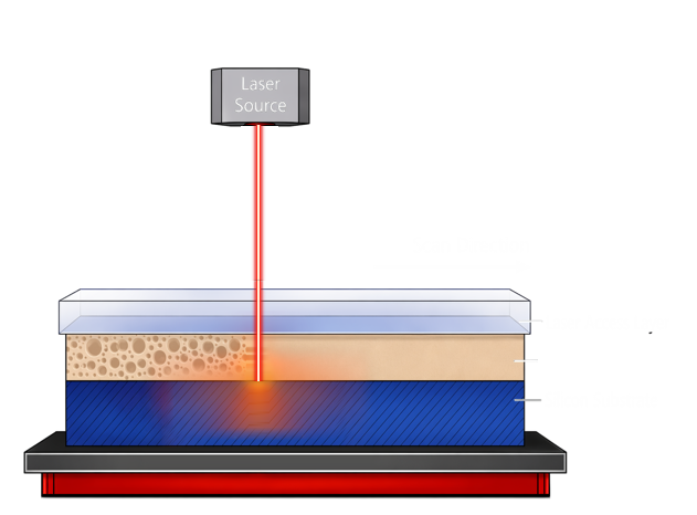
A patent-pending, direct-write laser process forms embedded porosity in place, beneath the surface of the wafer.
What It Produces
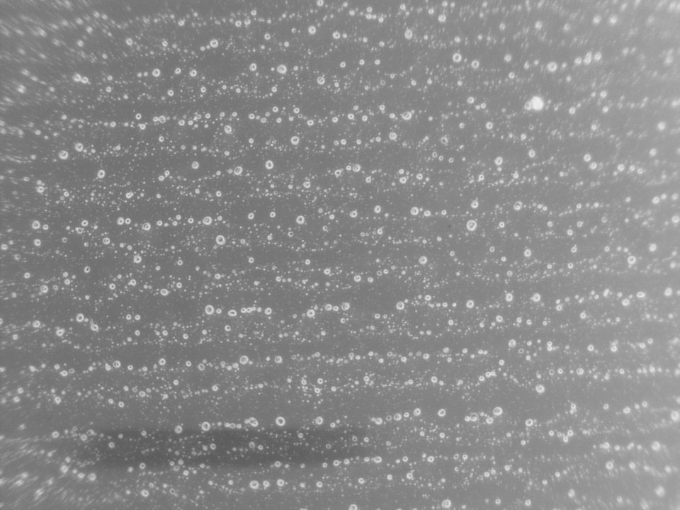
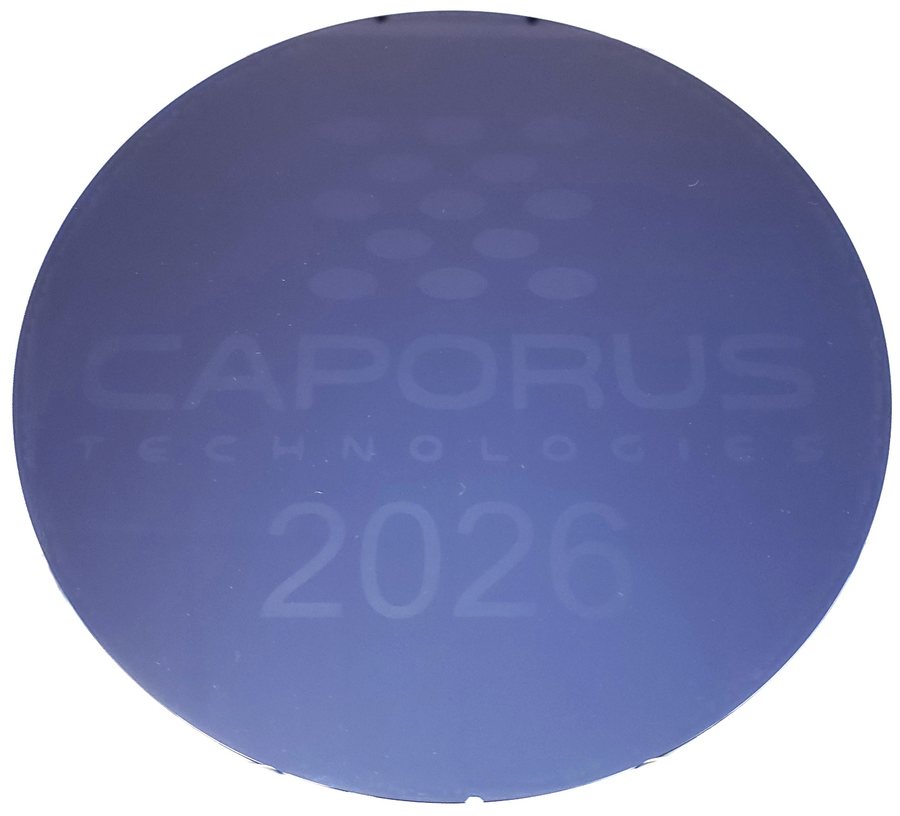
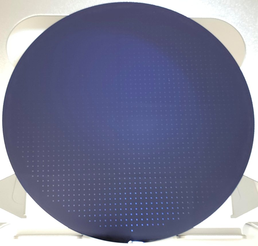
Sealed cavities form up to several microns below a continuous, intact surface. They can be written region by region or across entire wafers.
Proven Results
Laser-modified regions compared with unmodified control regions on the same substrate. RF testing of laser-modified wafers showed lower RF loss, higher effective resistivity, reduced H2/H3 harmonics, and reduced coupling and crosstalk, comparable to industry-standard high-resistivity trap-rich SOI at room temperature.

Independent third-party measurement. RF measurements were performed by Incize, an independent test laboratory.
Substrate Platforms
LMS™ technology is designed for layered and bonded wafer architectures.
Differentiation
LMS™ targets the RF linearity and loss of commercial trap-rich substrates, and adds the thermal budget and spatial selectivity that poly-Si cannot offer.
| Poly-Si Trap-Rich | Caporus LMS™ | |
|---|---|---|
| RF linearity and H2/H3 suppression | Yes | Yes |
| Low loss, high effective resistivity | Yes | Yes |
| Thermal budget | Limited (recrystallization) | Stable cavities to 1200 °C |
| Spatial selectivity | None | Directly writable |
| Operating temperature | About 100 °C | 125 °C and above |
| Substrate architecture compatibility | Limited | Broader |
| Ion implantation or deposition needed | Deposition (CVD poly-Si) | None |
| Technology | Ion Implant | P-N Junctions | Spatially Localizable | Thermal Budget | Oxide Planarity | Integration Complexity |
|---|---|---|---|---|---|---|
| Implantation-based defects and cavities | Yes | No | Yes | Limited | Preserved | High |
| Buried P-N junctions | Yes | Yes | Yes | Good | Preserved | High |
| Porous Si (electrochemical etch) | No | No | Limited | Limited | Often degraded | High |
| Caporus LMS™ | No | No | Yes | High | Preserved | Lower |
Applications
Starting with RF-SOI front-ends, with applications across advanced substrate platforms.

Antenna switches, tuners, and LNAs for 5G, 5G-Advanced, and Wi-Fi 6E/7

RF next to digital or photonic devices on one wafer, and chiplets

RF-optimized regions for low-loss, co-packaged optics

Monolithic active pixel sensors (MAPS) and quantum devices
Partner With Caporus
We are engaging partners on RF-SOI integration, GaN on Si, POI, heterogeneous integration, detectors, quantum, and new applications.
Share your platform and targets, and we will set up an evaluation against a shared benchmarking plan.